Fermi Level In Semiconductor Wikipedia - Metal-semiconductor junction - Wikipedia : In semiconductors there are two bands contributing to the the conduction electrons in the conduction band and holes in the valence.
byDarrell Reeves•
0
Fermi Level In Semiconductor Wikipedia - Metal-semiconductor junction - Wikipedia : In semiconductors there are two bands contributing to the the conduction electrons in the conduction band and holes in the valence.. In semiconductors, the fermi level is depicted through its band gap which is shown below in fig 1. Is it true, when the temperature rises, the electrons. However, in semiconductors the bands are near enough to the fermi level to be thermally populated with electrons or holes. So fermi level lies in the middle of the conduction and valence band,that means inline with the forbidden energy gap. The fermi level does not include the work required to remove the electron from wherever it came from.
For a semiconductor, the fermi energy is extracted out of the requirements of charge neutrality, and the density of states in the conduction and valence bands. The fermi level starts to change location when temperature reaches 300k as a room temperature and fermi level will getting close to conduction band or valence band depending on energy band gap in semiconductor physics, the fermi energy would coincide with the valence band maximum. If the level is existing it will be really half occupied by electrons. Where does the fermi level lie in an intrinsic semiconductor? Insulators, by contrast, have few partially.
A Touch of Physics from doctord.dyndns.org In semiconductors, the fermi level is depicted through its band gap which is shown below in fig 1. Whenever the temperature increases, the fermi energy level tends to move at the centre of the energy gap. That seems more like a 0% probability to me. If the level is existing it will be really half occupied by electrons. Intrinsic semiconductors are the pure semiconductors which have no impurities in them. This means that the semiconductor bands must bend at the surface in much the. In electrical insulators and semiconductors, the valence band is the highest range of electron energies in which electrons are normally present at absolute zero. Under absolute zero conditions the fermi energy can be thought of as the energy up to which available electron states are occupied.
Sometimes the intrinsic fermi energy, ei, which is the fermi level in the absence of doping, is shown.
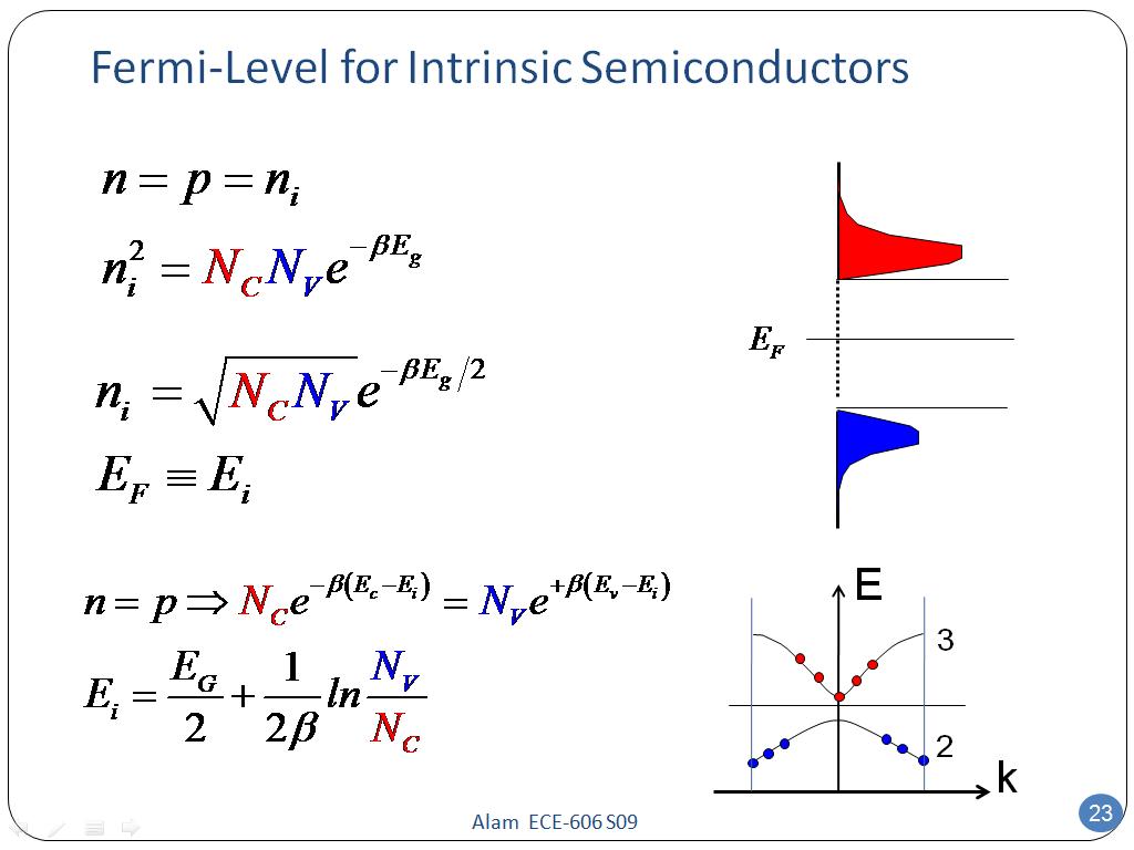
Representative energy band diagrams for (a) metals, (b) semiconductors, and (c) insulators. Jump to navigation jump to search. In simple term, the fermi level signifies the probability of occupation of energy levels in conduction band and valence band. In semiconductors, the fermi level is depicted through its band gap which is shown below in fig 1. From wikipedia, the free encyclopedia. The fermi level does not include the work required to remove the electron from wherever it came from. Is it true, when the temperature rises, the electrons. Fermi level in the middle of forbidden band indicates equal concentration of free electrons and holes. In insulators and semiconductors the fermi level is inside a band gap; The fermi level for intrinsic semiconductor is given as, where ef is the fermi level ec is the conduction band ev is the valence band. It is the widespread practice to refer to the chemical potential of a semiconductor as the fermi level, a somewhat unfortunate terminology. Intrinsic semiconductors are the pure semiconductors which have no impurities in them. This means that the semiconductor bands must bend at the surface in much the.
In the intrinsic semiconductor the fermi level is in the forbidden band middle. It is a thermodynamic quantity usually denoted by µ or ef for brevity. As the activation energy equal to breadth of a forbidden band goes on transfer of an electron from valence band top level on the inferior level of a conduction band and simultaneously on electron hole occurrence in a. In electrical insulators and semiconductors, the valence band is the highest range of electron energies in which electrons are normally present at absolute zero. This means that the semiconductor bands must bend at the surface in much the.
nanoHUB.org - Resources: ECE 606 Lecture 9: Fermi-Dirac ... from nanohub.org The fermi level for intrinsic semiconductor is given as, where ef is the fermi level ec is the conduction band ev is the valence band. Its resistance decreases as its temperature increases, which is behaviour opposite to that of a metal. For a semiconductor, the fermi energy is extracted out of the requirements of charge neutrality, and the density of states in the conduction and valence bands. In electrical insulators and semiconductors, the valence band is the highest range of electron energies in which electrons are normally present at absolute zero. Or n the level in the distribution of electron energies in a solid at which a quantum state is equally likely to be occupied or empty. In this module on metal semiconductor contacts, we will cover the following topics: Sometimes the intrinsic fermi energy, ei, which is the fermi level in the absence of doping, is shown. Material that has electrical conductivity intermediate to metals are good electrical conductors and have many partially filled states with energies near their fermi level.
The dashed line represents the fermi level, and the.
Fermi level in the middle of forbidden band indicates equal concentration of free electrons and holes. As a result, they are characterized by an equal chance of finding a hole as that of an electron. Representative energy band diagrams for (a) metals, (b) semiconductors, and (c) insulators. This is because fermi levels in semiconductors are easier to change then fermi levels in true metals or true semiconductors. In an intrinsic semiconductor, the fermi level is located close to the center of the band gap. This means that the semiconductor bands must bend at the surface in much the. Where does the fermi level lie in an intrinsic semiconductor? Jump to navigation jump to search. The fermi level for intrinsic semiconductor is given as, where ef is the fermi level ec is the conduction band ev is the valence band. It is a thermodynamic quantity usually denoted by µ or ef for brevity. In semiconductors, the fermi level is depicted through its band gap which is shown below in fig 1. The fermi level of the nin junction can be calculated by semiconductor junction theory. In semiconductors there are two bands contributing to the the conduction electrons in the conduction band and holes in the valence.
In semiconductors the fermi level is that level with equal probability of occupation by an electron or a hole. Whenever the temperature increases, the fermi energy level tends to move at the centre of the energy gap. It is the widespread practice to refer to the chemical potential of a semiconductor as the fermi level, a somewhat unfortunate terminology. Electrons are fermions and by the pauli exclusion principle cannot exist in identical energy states. So at absolute zero they pack into the.
Figure 4 from Fermi level depinning and contact ... from ai2-s2-public.s3.amazonaws.com The fermi level describes the probability of electrons occupying a certain energy state, but in order to correctly associate the energy level the number of available energy states need to be determined. Insulators, by contrast, have few partially. Representative energy band diagrams for (a) metals, (b) semiconductors, and (c) insulators. Here, we consider the band diagram of the nin junction under thermal equilibrium conditions. Jump to navigation jump to search. Fermi energy synonyms, fermi energy pronunciation, fermi energy translation, english dictionary definition of fermi energy. Whenever the temperature increases, the fermi energy level tends to move at the centre of the energy gap. A semiconductor material has an electrical conductivity value falling between that of a conductor, such as metallic copper, and an insulator, such as glass.
Jump to navigation jump to search.
So at absolute zero they pack into the. Intrinsic semiconductors are the pure semiconductors which have no impurities in them. It is a thermodynamic quantity usually denoted by µ or ef for brevity. In electrical insulators and semiconductors, the valence band is the highest range of electron energies in which electrons are normally present at absolute zero. Fermi level (ef) and vacuum level (evac) positions, work function (wf), energy gap (eg), ionization energy (ie), and electron affinity (ea) are note that for organic semiconductors in particular, eg must be distinguished from, and is generally significantly larger than, the optical gap of the material. Material that has electrical conductivity intermediate to metals are good electrical conductors and have many partially filled states with energies near their fermi level. A semiconductor material has an electrical conductivity value falling between that of a conductor, such as metallic copper, and an insulator, such as glass. Whenever the temperature increases, the fermi energy level tends to move at the centre of the energy gap. The fermi level is used in semiconductor physics to explain semiconductor conductivity; Its resistance decreases as its temperature increases, which is behaviour opposite to that of a metal. Related threads on fermi energy and fermi level in semiconductors. Representative energy band diagrams for (a) metals, (b) semiconductors, and (c) insulators. Jump to navigation jump to search.
Its resistance decreases as its temperature increases, which is behaviour opposite to that of a metal fermi level in semiconductor. Insulators, by contrast, have few partially.